
SU-8: Thick Photo-Resist for MEMS
since 01/1999, modified 05/2023
Introduction
We hope this page will eventually contain all the known data about the SU-8 photoresist. Thus, we need your help! Send all your data number 4480, and I will include it in this page, with credits, of course!The SU-8 is a negative, epoxy-type, near-UV photoresist based on EPON SU-8 epoxy resin (from Shell Chemical) that has been originally developed, and patented (US Patent No. 4882245 (1989) and others) by IBM. 
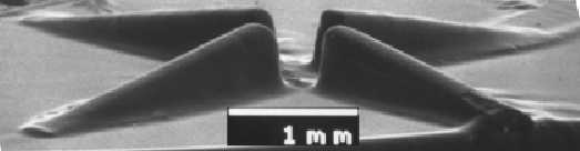
This photoresist can be as thick as 2 mm and aspect ratio >20 and higher have been demonstrated with a standard contact lithography equipment (picture courtesy of R. Yang).
These astounding results are due to the low optical absorption in the UV range which only limits the thickness to 2 mm for the 365nm-wavelength where the photo-resist is the most sensitive (i.e., for this thickness very little UV light reach the bottom of the structure).
Of course LIGA still yield better results but low-cost application will undoubtedly benefit from this resist that is well suited for acting as a mold for electroplating because of its relatively high thermal stability (Tg>200°C for the cross-linked (i.e., exposed) resist).
Two companies have now bought a license from IBM to sell the photoresist :
- Kayaku Advanced Materials (previously MicroChem Inc and Microlithography Chemical Corp.), 200 Flanders Road, Westborough, MA 01581 USA, Tel: +1 617-965-5511 under the name SU-8 ### with different viscosities (SU-8 5; SU-8 10; SU-8 25; SU-8 50; SU-8 100), the SU8-2000 ### where the standard GBL solvent is replaced by cyclopentanone and has improved wetting properties, and the SU8-3000 ### which boasts lower stress.
- Gersteltec SARL General-Guisan 26, CH-1009 Pully, Switzerland, Tel: +41 (0)79 564 34 23, Fax: +41 (0)21 728 35 83, under the name GM1040, GM1060, GM1070 (the reference are the same as used previously for Sotec Microsystem products) and GLM2060 for a SU8 with nanocomposite filler.
- There are local representative of these two companies everywhere. can be found on a separate page (if you want to appear on this page, just send an email)
Physical properties
Using the litterature reference, the following tables, based on an original compilation from Loren St Clair, gives some properties of the resist. We begin with the known mechanical properties:
| Characteristics | Value | Conditions | Reference |
|---|---|---|---|
| Modulus of elasticity : E | 4.02 GPa | in tension, postbaked at 95°C, screw tensile testing machine | Lorenz97 |
| 4.95 ± 0.42 GPa | hardbaked at 200°C, beam deflexion test | Dellmann97 | |
| 4.4 GPa | postbake at 95°C, SM blend | SOTEC MICRO | |
| 3.48 ± 0.57 GPa | hardbake, 2µm film | Robin13 | |
| 2.92 ± 0.43 GPa | no hardbake, 2µm film | Robin13 | |
| Bi-axial modulus of elasticity : E/(1 - n) | 5.18 +/- 0.89 GPa | postbaked at 95°C, thermal cycling test on Si wafer | Lorenz98c |
| Poisson ratio | 0.22 | postbaked at 95°C, SM blend | SOTEC MICRO |
| Film stress | 19 - 16 Mpa | for 0 - 400 mic. thick SU-8 film coated on a 3" 375 mic. thick Si wafer, prebaked, illuminated, postbaked at 95°C and brought back to room temperature (20°C) | Lorenz98c |
| Max stress | 34 Mpa | hardbaked at 200°C, lateral deflexion FEM analysis | Dellmann97 |
| Max sheer | 0.009 | hardbaked at 200°C, lateral deflexion FEM analysis | Dellmann97 |
| Plastic domain limit | 'no' plastic domain observed | hardbaked at 200°C, sample pulled until fracture | Lorenz97 |
| Friction coefficient : μ | 0.19 | postbaked at 95°C, pin-on-disc installation (10 g load) | Lorenz97 |
| Bond strength (see comments below) |
4.8 +/- 1.2 MPa | on Au, Instrom pull test | Nordstrom05 |
| 5.6 +/- 2.5 MPa | on Ti, Instrom pull test | ||
| 12.1 +/- 2.8 MPa | on Al, Instrom pull test | ||
| 20.7 +/- 4.6 MPa | on Si, pull test |
The next table gives data about physical properties of the polymerized SU-8:
| Characteristics | Value | Conditions | Reference |
|---|---|---|---|
| Glass temperature: Tg (see comments below) |
~50°C | unexposed film (not polymerized) | LaBianca95a |
| >200°C | fully crosslinked film (hard baked) | ||
| ~55°C | MCC blend before PEB | MCC | |
| Degradation temperature: Td (see comments below) |
~380°C | fully crosslinked film (hard baked) | LaBianca95a |
| Coefficient of thermal expansion : CTE | 102.0 +/- 5.1 ppm/K | SU-8 25 hard baked at 200°C for 10 min (in-plane). | Feng02 |
| 52.0 +/- 5.1 ppm/K | SM10#0 postbaked at 95°C, thermal cycling test on Si wafer | Lorenz98c | |
| 30 ppm/K | SM2050 with 50% filler in the blend | SOTEC MICRO | |
| 21 ppm/K | SM2070 with 70% filler in the blend | ||
| Thermal conductivity | 0.2 W/mK | general value for thermoplastic not for SU-8 | Guerin97 |
| Specific heat | 1.5 kJ/kg K | source not specified | Elali04 |
| Polymer shrinkage | 7.5% | postbaked at 95°C | Guerin97 |
| Density: ρ | 1200 kg/m3 (or 1.2 g/cm3) | Density of the raw SU8 resin (not for the PR) | Resins.com |
| Viscosity (Dynamic or Absolute): η or μ | 0.06 Pa.s = 6 cP | SM1040 (40% solid + GBL), DIN53019 | Lorenz97 J-L Guerin. |
| 1.5 Pa.s = 1500 cP | SM1060 (60% solid + GBL), DIN53019 | ||
| 15 Pa.s = 15000 cP | SM1070 (70% solid + GBL), DIN53019 | ||
| Kinematic viscosity: ν (we have ν ρ= η) | 0.000045 m2/s = 45 cSt | SU-8 2 | MCC |
| 0.000290 m2/s = 290 cSt | SU-8 5 (52% solid + GBL), density 1.1641, 20°C | ||
| 0.001050 m2/s = 1050 cSt | SU-8 10 (59% solid + GBL), 20°C | ||
| 0.0025 m2/s = 2500 cSt | SU-8 25 (63% solid + GBL), 20°C | ||
| 0.01225 m2/s = 12250 cSt | SU-8 50 (69% solid), 20°C | ||
| 0.0515 m2/s = 51500 cSt | SU-8 100 (73% solid), 20°C |
And this table gives data about the electromagnetic properties of the polymerized SU-8:
| Characteristics | Value | Conditions | Reference |
|---|---|---|---|
| refractive index: n | 1.67 | at 365 nm, not crosslinked (during exposure before PEB) | MCC |
| 1.67 | at 408 nm, idem | ||
| 1.596 | at 633 nm, crosslinked PR after proton beam exposure, prism-coupling technique | Sum03 | |
| 1.575 | at 1550 nm, idem | ||
| 1.7 | at 1.6 THz, postbaked at 100°C (+8 hours at 65°C in KOH), THz time domain spectroscopy | Arscott99 | |
| 1.8 | at 100 GHz, idem | ||
| absorption coefficient: α | ~2 cm-1 | at 100 GHz, postbaked at 100°C (+8 hours at 65°C in KOH), THz time domain spectroscopy | Arscott99 |
| ~40 cm-1 | at 1.6 THz, idem | ||
| loss tangent: tan δ | 0.08 | at 100 GHz, postbaked at 100°C (+8 hours at 65°C in KOH), THz time domain spectroscopy | Lucyszyn01 |
| 0.14 | at 1 THz, idem | ||
| relative dielectric constant: εr | 4 | at 10 MHz, postbaked at 100°C, may be valid between 20 GHz and 40 GHz | Thorpe98 |
| 4.5 | at 10 MHz | James Thorpe | |
| 4.2 | at 10 GHz | ||
| 3 | at 10 MHz, postbaked at 95°C, SM blend | SOTEC MICRO | |
| Breakdown voltage | 1.1 105 V/m | electrical breakdown 1.2V for an 11 μm thick SU8(10) film | James Thorpe |
| >4 107 V/m | electrical breakdown did not happen at 1000V for a 25 μm thick SU8 film | Eric Codner | |
| 4.43 ± 0.16 108 V/m | SU-8 2 and SU-8 in the range of 2-15 μm | Melai09 |
Other properties
Here are some general properties that can not fit in a table, and are deducted mostly from experiment. They should not be taken for more than that :-)
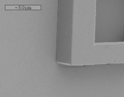
- Aspect ratio larger than 1:50 has been obtained... but repeatability may be a problem :-) Typical aspect ratio would be 1:20, and 1:25 for good process (picture courtesy of R. Yang).
- It is possible to perform gray tone lithography with SU8 (see process below).
- Using MeV proton beam iradiation (instead of UV) the aspect ratio can go up to 100. In this case the exposure dose should be about 10-40 nC/mm2 for complete irradiation. Note that the MeV protons are almost not absorbed by the SU8, nor reflected by the substrate, which helps a lot in getting large aspect ratio! [Sum Tze Chien, NUS]
- The chemical resistance of SU-8 is quite excellent however most chemical etches it, albeit at a very slow rate. This very slow rate create diverging report for the etching resistance of SU8 and to avoid further confusion, we will report the chemical resistance only with an etching rate - currently none is known, but to give an idea of how difficult it is to etch it away, one week in H2S04 at room temperature for removing 100um layer is the kind of speed we are looking for :-) Moreover some person consider peeling of SU8 as 'etching', adding to the confusion...
- Adhesion of SU-8 is usually good, but depends on the material. The adhesion is worst with gold (Au), average with silicon with native oxide, and best with silicon nitride (SiN) [Frank].
The adhesion of SU-8 seems to be affected by the chemical and SU-8 lift-off with immersion in KOH and TMAH, whereas it sticks with HF [unfortunately no detail available about the substrate]. As adhesion problem are linked with substrate cleanliness, those reports are to be taken with a pinch of salt :-) Finally, MCC with the newer SU-8 2000 series, claims a better adhesion on most materials, due to the change of solvent. Thank you to those who contributed!
We have some experience with Al magnetron sputtering on SU8. In order to get a good adhesion there should be a very effective Sputter Etch step before Al sputtering to activate the surface of SU8 [David Ovrokzky] Thank you David!. - SU-8 seems to have a good biocompatibility. In collaboration with neuroscientists working in the domain of electrophysiology, they use to culture biological cells on SU-8 and it seems that there is a 'good' biocompatibility of this material. The SU-8 photoepoxy is used as passivation layer for measurement electrodes in the bottom part of a cell culture chamber. [Marc Heuschkel, EPFL]. Thank you Marc!
- The SU-8 is very difficult (impossible?) to reflow when it is cross-linked. At 210°C it does not reflow after 21h (!) but at 220°C it already changes colour and turns black... [Ren Yang] Thank you Yang!
The glass transition temperature of SU-8 after crosslinking is approximately 230°C, but don't expect much to happen [confirming above behaviour which is different from a positive PR]. Because the density of crosslinking in SU-8 is very high, there is not much change in the film after processing, even at high temperatures. Shrinkage will occur to around 350°C with the maximum change occurring before 270°C. After that a 5% weight loss is noted at 364°C with the char temperature being 900°C [Rob Hardman, MicroChem]. Thanks Rob for these additional information!
My experience with a sample with submicrometer features, heated in a non-oxidizing (argon) atmosphere:- 300°C, no problem
- 350°C, a few hours
- 400°C, a few minutes
- ~300°C, small amounts of uncrosslinked monomers (equivalent to an "SU-2") come off
- ~450°C, major structural degradation
I baked cross-linked SU8 to 400°C for 20mins. It turned dark brown, and the center sagged. The structure turned out to be a little less robust. It can shatter if you scratch VERY hard with a tweezers. The CD at the bottom didn't change, but the profile tapered to about 105 degrees. [ShuTing Hsu, UCLA] Thanks ShuTing!
Process Tips
Here are all the data gathered over the years pertaining to the SU-8 processing. These datas complete the general information you may obtain from the literature, and are mostly tricks. But they do help a lot :-) Contact in bracket gives the source of the info. The text is almost verbatim from the source, with only very slight edition when it was needed. When some details are 'not available', it is mostly because of some proprietary information that could not be divulged openly. Sometimes, SU-8 processing looks more like an art than like an exact science :-)- MicroChem Corp., one of the SU-8 manufacturer, provides good process sheets that usually is a reasonable strating point. You may also want to have a look at their FAQ dedicated to SU-8. A good source of information...
- Now defunct SOTEC MICROSYSTEM had compiled a lot of interesting trick about the processing of the SU-8 which are now (partly) available through Dr J. L. Guerin homepage. For example they used to explain that the thin solid crust that is often observed when dealing with thick layer of photoresist, causing loss of resolution, is due to the heating of the surface induced by high dose (200 mJ/cm2) and long exposure time. A way to alleviate the problem is to divide the exposure in 10 to 15 seconds intervals with a 60 seconds waiting time in between. Of course, as with other photoresist, the exact exposure time is shown to depend on the substrate reflectivity, but, in most case, a bit of over-exposure is not a problem here (negative resist).
- EV group (formerly Electronic Visions) has compiled another interesting document on the SU-8 processing describing a complete process in details, with thickness (10 µm - 450 µm) versus spinner speed (300 rpm - 1500rpm) charts for all commercial blend of SU-8 (SU-8 5 to SU-8 100), pre-exposure time versus thickness (from 30 min at 10 µm to... 7 hours at 450 µm!), exposure (broad band UV source 350 nm - 450 nm) dose versus thickness (from 150 mJ/cm2 (measured at 465 nm) at 10 µm to 1400 mJ/cm2 at 450 µm) and some useful tricks. The document is in PDF format... but too big to include on this page. It is not on their website but you may ask Chad Brubaker for the application notes on SU-8. Meanwhile, here is a short extract, the table of layer thickness at a spin speed of 900 rpm for the different blend of SU-8 (static dispense, about 1ml of SU-8 per inch diameter of the wafer to coat, ie 4'' wafer = 4 ml) [Eva Wimmesberger] :
SU-8 Thickness (µm) 5 12 10 30 25 58 50 150 100 320 - A complete process example with 70% solid resist (equivalent to GM1070) [S. Basrour, J.-C. Jeannot & V. Soumann, LPMO/CNRS, IMFC, Universite de Franche-Comte, Besancon, France, Translated from French: F. Chollet]. Thank you Skandar!
Spin-Coating
(130 µm layer)speed = 1500 rpm
acceleration = 100rpm/s
duration = 60 sSoft bake 30 min at 95°C Relaxation time wait 10 min Exposure 165 mJ/cm2 (with a standard contact UV aligner for microelectronics) Post bake 15 min at 95°C Relaxation time wait 10 min Development place the sample in pure PGMEA (propylene glycol methyl ether acetate) during 5 min
rinse with isopropanol (IPA)
if some white stains remain, replace sample in PGMEA for 5 min
repeat until no more white stain appearRemarks The photo-resist is VERY SENSITIVE to the planarity of the devices used during the whole process (hot plate, UV exposure(?)...) (e.g., reflow occur on the hot plate) and for good results, the equipment has to be carefully leveled. The photo-resist is very hard to strip after cross-linking. The exposed photo-resist soften during hard bake while the non-exposed photo-resist remains hard (?). The side walls are 'very' smooth and 'vertical'. - Spinning
- To remove bubbles from SU-8 prior to spinning, the resist can be heated to lower the viscosity and allow bubbles to float to the top. Note that resist should be allowed to cool to room temperature before spinning. Although this worked to remove the larger bubbles, we still observed microbubbles after 30 minutes at 60 degrees C. Our current process is to put the resist into a Norm-Ject syringe with cap, pull the plunger and fill from the back side, replace the plunger, purge large bubble, and centrifuge. At room temperature the resist had no visible bubbles after centrifuging for 15 minutes. [Mathew Lewis, Ingenuity-K]
- For easier (manual) dispensing pour the most viscous SU-8 (2050+) directly from the bottle. Forget the pipette [Henry Yang, IBM]. A good point Henry!
- To remove the bubbles and have a nice even coating, place the wafer on a hotplate @ 30- 35 deg C and pour SU-8 2050 over the wafer, wait for a second or two, the SU-8 becomes flowy enough to remove the (bigger) bubbles, remove the wafer from the hotplate swivel the SU-8 across the wafer, then place the wafer on the spin coater and follow your usual recipe [Aarthi Lavanya Dhanapaul, NUS].This trick presumably works with the largest bubble, but it is simple to apply!
- To avoid streaks on wafers, one method that seemed to work for us was to squeegee a thin layer of SU-8 across the entire substrate. Then immediately add more resist in the center, the usual amount, and spin. A quick and dirty solution, but it worked for us and kept my substrates from looking like spin art. Best of luck to you [Dara Ruggiero, Harris]. Why not Dara!
- A technique used to minimize the quantity of resist dispensed on a wafer is to pre-wet the wafer with the solvent - not dry completely then dispense and spin. One of the resist companies did some work on it if I recall correctly. You can understand why they would not publicize it much. I don't know how it would work if you have very large topography but it may be worth a try [Avi Laker, Teccor Electronics]. Sounds very interesting Avi!
- When you apply the SU-8 have the wafer rotating about 20 or so rpm to get a puddle that is centered every time. You may have to change the slow spin rpm for 2" wafers. Also, start the spin cycle at a slow acceleration, say 200 rpm per second [Clifford J. Hamel, Suss Microtec]. Thanks Cliff!
- Use of high acceleration to ramp up to spin off speed. I know that this is contrary to what some others on the group have said, but the principle of the high spin off makes sense. The reason for the "starfish" pattern has more to do with the surface tension of the resist than of its viscosity. Basically, once a "tendril" of resist has made it to the edge of the wafer, the path of least resistance for the flow of resist is within that "tendril", since the surface tension of the walls of the "tendril" is so high.
By using high acceleration (>10,000 rpm/sec, ideally), there is a greater amount of force present to draw the resist outwards on the wafer. Additionally, the rapid acceleration motion breaks up the surface, allowing smoother flow [Chad Brubaker, EV group]. 'Contrary to popular belief' - I like that Chad! - Try placing a lid on after dispense before spinning and shut off your exhaust at the same time. There are various valves like one from a company called Progressive Technologies. This will allow the thick resist to spread without loosing too much of its solvent. Use a 400 rpm spread speed and then ramp to the final spin speed for whatever thickness you desire [Bob Henderson]. Thanks Bob!
- It is observed that the thickness of SU8 film has a tendency to increase after the expiry date on the bottle has passed. This is mostly due to the evaporation of the solvent that makes the resist more viscous and hence thicker. Try increasing the spinning speed or change your porocess parameter to accomodate the larger thickness if you want to avoid problems - of course if you can afford it, use a fresh bottle :-) Another factor affecting the viscosity is the temperature and it may take some time for the PR to reach the temperature of the room as it is usually stored in a fridge.
- Soft-Baking
- For high aspect ratio imaging, try longer soft bake times in order to reduce the retained solvent level. This may help since you will probably need to have longer develop times. By reducing the solvent level you reduce the risk of exposed resist loss, swelling, adhesion failure, etc. (However, for low aspect ratio structures it is often desirable to work with a bit more solvent, since it speeds up the development time and makes the film easier to strip.)[Scott Heidemann, MicroChem Corp.]. Thank you Scott!
- it has been reported a few times that the best way to bake the SU-8 (and the `official' MCC way) is to use a hotplate. Although some people have reported success in using an oven it is suspected that the baking from the oven will form `crust' on the SU8 surface that has a low solvent concentration that would slow down the evaporation of solvent in the bulk. With the hot plate the baking from the bottom seems to provide the temperature gradient helping in the diffusion/evaporation of the solvent. For the temperature and duration... ask your witch-doctor!
- The SU8-2000 series from MCC is using cyclopentanone as the solvent instead of GBL in their standard SU8 and in Gersteltec formulations. This has a significant impact on the backing duration to evaporate the solvent and was the main driver behind the development of this new photoresist. For example for a 100μm thick film the recommended soft-bake time drops from 40mins to 25mins. It is even better for thinner film and a 50μm thick layer soft-bake drops from 26mins to 9mins. The PEB is apparently (and logically) not modified.
- During soft-bake it has been regularly reported that craters or divots can form on a film which appeared normal after spin-coating. From the report, it is suspected that the origin of the crater is from some surface contamination. the general solution seems to be to better clean (and rinse!) the wafer before spinning.
- I've read other reports of this happening, and it's happened to me at times as well on glass substrates. We have overcome this somewhat with longer pre-exposure bakes at a lower temperature (85°C). I've also found a prebake of my glass substrates is essential for good adhesion. [Jon R. Fox]. The longer prebake of the substrate is probably helping too... Thanks Jon!
- I suspected contamination of the substrate during my cleaning process. I normally use conc. H2SO4 for cleaning (although the datasheets do recommend piranha, this needs to be made fresh every time and is quite wasteful). The problem was resolved after changing my H2SO4.[Gareth Jenkins]
- Waves or wrinkles may also appear during the soft-bake and their origin has been traced back to:
- I had some time a similar problem and the conclusion was that the hotplate temperature was not completely uniform [GARCIA BLANCO Sonia]
- The waves will appear if the surface of the SU8 bakes faster than the inner regions. This will always happen in any baking regime of course, and is the reason why SU8 users opt for hotplates rather than convection ovens (the latter encouraging surface drying and skin formation, preventing solvent evaporation from deeper planes within the film). If by 'waves' you mean 'wrinkles' then it looks like the surface is in fact drying much faster than inner regions; preventing the required levels of soft baking / film hardening. My advice is twofold. First, try to spin a layer with half the thickness and cure with the same parameters. If there are fewer or no waves, then it would suggest that solvent evaporation is responsible for the problems you are seeing. Then (second) extend your softbaking time at BOTH 65°C and 95°C for your desired SU8 layer thickness. Another thing you could try is to place a petri dish over (and not touching) your coated wafer on the hotplate, standing on glass slides to allow solvent escape. This will help to retain some solvent over the surface layer, slowing its drying rate and homogenising the overall drying rate of the film. This is after all what you are aiming to do by having a two step baking process. The general rule to follow if your film is not uniform is to take measures that reduce temperature and evaporation differentials between surface and inner regions of the SU8 film. The more you can homogenise your curing process (including exposure) the more uniform your film properties / thickness will be. [Michael Larsson]
- Sticking quite often, the SU-8 layer sticks to the mask during exposure (collected by Paddy on the MEMS-list).
- Even we had this problem of mask sticking. It mainly relates to prebake. We do prebake in a oven (not hot plate) at 90°C for 25 to 30 mins. We leave it for at least 10-15 mins in air before exposing it in the mask aligner. That appears to work alright. We never had the problem of cracking. It appears that the resist is under stress for some reason in your case. You may need to optimise the exposure and PEB times.
- I had trouble with a ridge all around the wafer, that was thicker and sticky. I had to remove it 'manually' in some cases... but I believe you don't have this problem. With thick photoresist (not SU-8) I used to simply cover the wafer with a half petri dish on the hot plate, the increased baking (ie, IR get reflected) on the resist surface (remember a hotplate bake sample from the bottom) was sufficient to suppress sticking problem I experienced previously. Alternatively, you may wish to try a convection oven for the softbake, it bakes the sample more uniformly.
- Exposure
- Different people reported what is refered as a T-topping with SU-8 when it is processed with wideband UV source. The reason seems to be in the high absorption of the SU-8 at wavelength shorter than ~350nm, if you use such wavelength, the top layer is strongly exposed (a lot of acid is generated that diffuse), while the bottom part is not. A cure to this problem is to use a filter to cut down the wavelength below 350nm. For example a Hoya UV-34 filter, 2.5mm thick (transmittance: 0% at 325nm, 50% at 350nm, >80% at 370nm and above), was used in a Quintel Q7000 mask aligner, and did provide the very clear following results [Steven Hobson, FraunhoferUSA]. Thank you Steve!
Without the UV filter With the UV filter (Hoya) 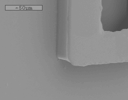
- Another reason for T-topping may be where amine and airborne contamination levels are not controlled, that may result in surface contamination that get 'amplified' by the photoresist. This seems to be more critical when pattern 1um or below ar targeted. Please contact the reporter if you observed this effect! [Inna Mushkatinskaya, Anvik Corporation]. Thanks Inna!
- SU-8 absorbs MUCH more at 320 nm than at 365 nm [...] thus 320 nm lasers should not be used for SU-8 exposure, unless it is for very thin layers. [Jacques Jonsmann] Good and valid point, thanks Jacques!
- When you reduce the solvent level (by using longer soft-bake) you may need to increase your exposure dose.[Scott Heidemann, MicroChem Corp.]. Thank you Scott!
- The exposure dose stated (in the datasheet) is for Silicon as a substrate and when it is used on a seed layer (for electroplating) the dose required can be in the range 1.5 - 2 X the dose required for Si. [Mark Shaw, MicroChem Corp.]
- Different people reported what is refered as a T-topping with SU-8 when it is processed with wideband UV source. The reason seems to be in the high absorption of the SU-8 at wavelength shorter than ~350nm, if you use such wavelength, the top layer is strongly exposed (a lot of acid is generated that diffuse), while the bottom part is not. A cure to this problem is to use a filter to cut down the wavelength below 350nm. For example a Hoya UV-34 filter, 2.5mm thick (transmittance: 0% at 325nm, 50% at 350nm, >80% at 370nm and above), was used in a Quintel Q7000 mask aligner, and did provide the very clear following results [Steven Hobson, FraunhoferUSA]. Thank you Steve!
- Post Exposure Bake (PEB)
- Some SU-8 users report that extended PEB times at lower temperatures produce better results than shorter times at higher temperatures. Some even go as low as 60°C in a convection oven. Other suggestions include ramping the temperature up, or starting at a lower initial temperature (around 50°C). The Tg of SU-8 before PEB is about 55°C, the idea is to produce some cross-linking prior to your primary PEB temperature which is frequently between 90-95°C, in order to prevent flowing. You might also consider ramping the temperature down after PEB to reduce stress and cracking.[Scott Heidemann, MicroChem Corp.]. Thank you Scott!
- Development
- Regarding the SU-8, I have developed in acetone, which works just fine for material removal. The biggest issue is that, when drying the acetone, it absorbs so much heat that the temperature of the substrate significantly drops, causing quite a bit of thermal-expansion (or in this case, contraction) stress to the film. It is very likely that any interior corners of your pattern will show evidence of stress cracks [Chad Brubaker]. Thanks Chad!
- Many SU-8 users have commented that this was their most challenging process step. For high aspect ratio features it is necessary to use medium to strong agitation. One SU-8 user reported that he actually suspends his wafer on a stir rod and immerses it in a beaker of developer. This gives him the best results (clears out deep vias and trenches). Obviously this isn't a high volume production worthy process, but may be helpful in a lab. Also consider using GBL, the SU-8 solvent as a predip prior to immersion in PGMEA. GBL is more aggressive than PGMEA and may clean up your sidewalls since it will remove partially cross-linked SU-8. I would recommend no more than 2-3 minutes, then go immediately into PGMEA. One word of caution; if you are under cross-linked GBL will chew up your structures. Another idea is to consider megasonics. This technique is commonly used in x-ray LIGA processes and has been reported to work well with SU-8.[Scott Heidemann, MicroChem Corp.]. Thank you Scott!
- Rinsing
- After the prescribed (by a registered Voodoo doctor) development time, I rinse the front and back side of the wafer w/ fresh PGMEA (MicroChem Developer), blow dry the back side, put it back on the spin coater, pool more PGMEA on the frontside and spin dry at 2-3 kRPM for about 15 seconds. You can actually watch as it dries. This seems to do a very good job at removing any excess solvent and thus any suspended polymer [Thomas Long, Georgetown University's Physics Dept]. Thank you Thomas!
- I'd be interested in hearing more on this subject. We have had no success with IPA or DI water. IPA seems to create white spots, which can not be subsequently removed in PGMEA. IPA may also cause surface cracking due to the high evaporation/cooling rate. DI water seems to be death. Any ideas? [Scott Heidemann, MCC]. Thank you Scott!
- Removing
- Since 2008 it seems that the best way to remove cross-linked photo-resist is to use the Muegge (previously R3T) remote plasma equipement. Removal rate may reach 20μm/min (more common rate on full wafer is 4μm/min) by isotropic etching with oxygen radicals without damaging metal or other material on the wafer [Muegge/R3T]. It is used by Mimotec with success since that time and received their prize for "best tool for SU8 removal" [Hubert Lorenz, Mimotec]. Thanks Hubert for the testimony !
- Uncross-linked SU8 photoresist can be removed with Acetone or PM Acetate before it harden
- The easiest way to remove cross-linked SU-8 is often to lift it off. As such, you can use a cheap sacrificial layer obtained by dissolving a polystyrene sheet in toluene and is removed with toluene. Have a look at the paper below.
- I have used the Microchem XP-adhesion/release layer [omnicoat]. I have only used it a few times so far but it works well. I noticed no difference with the adhesion (The SU-8 has not lifted up in the few PDMS molds I have made) and when I removed it, the 50 micron features started to lift off after a minute in PRS, and the wafer was clean in an hour of hot soaking [Glen Landry, NRL].
- Since 1996 at the EPFL and since 1998 at Mimotec we have tried almost all the solvents you can imagine (also the product of SOTEC) and i can say that nothing works. Mainly the people think they dissolve SU-8, they only remove it from a naked wafer. After plating it's smthg else.... (In our experiment) the SOTEC remover for SU-8+nickel has dissolved 40% of the nickel! [Hubert Lorenz, Mimotec] Thanks Hubert!
[Note that this is the only observation from a user of the remover from the now defunct SOTEC. Actually Mimotec was offering a cash prize to anyone providing a remover that fill their requirement, and it has been given to R3T, now Muegge for their plasma machine] - Now defunct SOTEC microsystem had a serie of liquid removers the SMST-S/M/H that could remove cross-linked SU-8 without affecting metals (the different version S, M or H of the SMST remover depends on the existing metals on the structure, the S version for Cu structure is very slow).
- A detailed study from Sandia lab among their LIGA related studies explore different ways of removal : solvent (<100°C), RIE (50% O2/50%CF4), molten salt (>300°C) - nothing revolutionary, but may be the best that can be done!
- Pirannah (H2SO4:H2O2) does attack SU-8 and can be used to strip even severly hardbaked films where solvents fail - if the substrate allows (Pirannah attacks a lot of other stuff as well). Another way to strip SU-8 is plasma containing Hydrogen radicals. We use NH3 as precursor, but pure Hydrogen (e.g. from forming gas) should also work [FB]. Thank you!
- ashing of the photoresist at a temperature larger than about 600°C leaves very few residue... if the structure can sustain it!
- SU-8 is virtually insoluble in most chemicals if well crosslinked. You would have to use RIE to etch off the SU-8. However only O2 Plasma does not work well. Try including 'some' CF4 (details not available :-). One thing that was observed is that if you have metal with SU-8 (cured at 200°C) SU-8 is removed without any CF4. Generally you are able to remove SU-8 with O2 plasma and CF4. Then the wafers go through an ultrasonic scrub clean to remove residues.[Paddy]. Thank you Paddy!
- O2 plasma alone does not work well but by introducing F-radicals (SF6 or CF4) different authors could report etch rate of several μm/min.
- I have etched SU8 (crosslinked) using RIE O2 99sccm [that's high!] and SF6 5sccm with 500W you get around 0.75μm/min. You need the SF6 to help etch the Silane groups that are in the SU8, otherwise you get a surface full of black dots and it is very rough.[Rick Morrison]. And here are some figure to start your process, thanks Rick!
- Adhesion and Cracks
- Cracking often appears after PEB (collected by Paddy on the MEMS-list).
The problem of the cracks is due to internal stress and is due to:
1) unsufficent exposure dose. Try to expose the layers with increasing dose: 10 mJ - 100mJ - 1000mJ. You will see that the quality of the surface change.
2) the cracks are due to the shrinkage of the SU-8. This effect is increased by exposing large areas of the wafer but if you adapt the design of your mask it disappears. - The PEB temperature is an important factor inducing stress and thus resposnible for cracks. The PEB temperature can be reduced to 55°C (instead of the 'official' 95°C) - but of course the PEB duration has to be increased substantailly (see paper).
- Defunct SOTEC MICRO had a blend of SU-8 with a filler that effectively reduce the coefficient of thermal expansion of the photoresist from 50ppm/K to 21 ppm/K. This brings it closer to the CTE of glass (about 10 ppm/K) and should decrease the stress related to CTE mismatch, thus allow for fewer cracks.
- I had a lot of adhesion problems and lifting of the SU8 during the development step and finally, the solution, was to ramp up and down all the hotplate steps. This really reduced the stress of the layers and therefore the lifting of the patterns. The hardbake could also induce further stress, I observed it myself! [GARCIA BLANCO Sonia].It is often said but easy to forget, thanks Sonia for reminding!
- Using SU8 as a mask to etch silicon in KOH usually fails because the KOH is able to dissolve the bond easily. The problem has been solved in some way by M. Larsson using interlocking structure.
- Adhesion of SU8 depends on the material (cf. Table above) but can be improved in general by either modifying the surface of the substrate or by reducing the interfacial stress during the process :
- depositing an underlying layer of metal with good adhesion property to SU8 (Al, Ti)
- using some adhesion promoter - but take care with HMDS, it may make the things worse. For glass or oxide a promoter that seems to work is the AP300 from Silicon Resources in Chandler, AZ. An example of the AP300 effect is shown below [Chad Brubaker]:
Glass adhesion without AP300 Glass adhesion with AP300 
- I've tried AP300 but have seen limited improvements to SU-8/substrate adhesion relative to other forms of chemical adhesion promoter. If you are using HMDS, try to repeat your process but ensuring the wafer is dehydration-baked at 150°C for 20-30 mins after HMDS application and prior to SU-8 spinning. If there is any moisture on the wafer pre- or post- HMDS application, this will hydrolyse the trimethyl substituted groups from the HMDS, reversing the process of silylation. In fact, removal of the HMDS substrate monolayer is achieved by rinsing in water. Applying HMDS in a humid environment worse for adhesion than not using any form of (chemical) adhesion promoter. Blowing nitrogen over your wafer surface (post HMDS) just before applying SU-8 would also be beneficial.[Michael Larsson] HMDS may not be that bad after all... Thanks Michael!
- increasing exposure dose [Maria Nordström] It has been reported many times, the data sheet dose given is for a certain substrate, mask, etc and yours is probably different - you'll often need a longer exposure time to get good exposure at the SU8/substrate interface a must to have good adhesion. Thanks Maria to point this not so obvious point!
- using a longer PEB (hours) at lower temperature (65°C or even 55°C) to avoid excessive stress. Some structures I bake at 60°C for 12 hours, then switch off the hotplate and allow it to cool down slowly. This is mandatory if the development process takes some hours. [Peter Svasek]
- Cracking often appears after PEB (collected by Paddy on the MEMS-list).
- Gray-tone lithography
- A method for fabricating structures in SU-8 photoresist having smoothly varying elevations has been developed at U. of Washington by M. Afromowitz team. Gray-scale structures up to 1 mm in height may be fabricated with one exposure step. Unfortunately the need for non-disclosure agreement prohibits to give detail on the method here, but contact the team with your application they will love it! [M. Afromowitz, U Washington] Thank you Marty!
These exceedingly linear SU-8 ramps (transparent in visible light, but opaque in this SEM) have lengths of 2.6 mm and maximum elevations of 0.5 mm (Viewed at 75° from the vertical direction).
- A method for fabricating structures in SU-8 photoresist having smoothly varying elevations has been developed at U. of Washington by M. Afromowitz team. Gray-scale structures up to 1 mm in height may be fabricated with one exposure step. Unfortunately the need for non-disclosure agreement prohibits to give detail on the method here, but contact the team with your application they will love it! [M. Afromowitz, U Washington] Thank you Marty!
Research Links
Here is a list of further links to more information on research done with the resist. Enjoy.- MCC is having a whole bunch of application notes (mainly on SU8 removal) and a few reference material on improving and using SU8.
- If you really want to reach large aspect ratio (up to 100) instead of using UV exposure you may want to use a proton beam using a maskless method. The group of F. Watt in Singapore has developped a whole lot of interesting stuff using SU8 (and other) and a proton source is not that expensive (at least much less than a synchrotron).
- Sporian Microsystem has a bulletin board dedicated to SU-8. I hope, because it is not attached to any SU-8 vendor but just to one user, that this forum will allow to start a real discussion of issues and trick on the SU-8, for the benefit of all! Note that you don't need to register, so, participate, now! (I hope it will be more active than the now defunct group established by MicroChem... or we will end by setting our own BB : actually, with the facility of the new server, we finally did it :-)
- The MEMS-talk list, is a good discussion group where you can ask for everything you want about MEMS and specially about SU-8.
- Here is a link to a paper from the original IBM team working on the SU-8 (albeit the original use of the SU-8 is for high resolution patterns and hence for very thin layers)
- The EPFL/IBM team SU-8 page with a lot picture to convince you to use the SU-8... or to simply use their technology for your molding or microfluidic application [Hubert Lorenz, MIMOTEC]
- An EPFL/Faculty of Medecine team has interesting results for biological (and example of different cell cultutre grows on the SU-8) and buried microchannels applications [Marc Heuschkel, EPFL]
- The old SOTEC Microsystem webpage, with very interesting processing tips, details about the chemistry and much more is back. [Louis J. Guerin, ex SOTEC]
Bibliography
Further very useful information (and the previous one :-) from the IBM and the EPFL teams (and a few others...) may be found in the following papers (please contact us if you know other references - specially historical ones :-) This list was established with the help of Loren St CLAIR, Hubert LORENZ, Arnaud BERTSCH, Marc HEUSCHKEL, Patrick MOUNAIX, LING Zhong-Geng, Stepan LUCYSZYN, SUM Tze Chien, Paul DENTIGER, ZHANG Jun, YANG Ren, TEH Weng Hong and David WOOD (it is available as a BibTex database).
- D. Stumbo and J. Wolfe, "Ion exposure characterization of a chemically amplified epoxy resist", J. Vac. Scien. Technol. B 11 (1993) : 2432-2435 [an early paper for those interested in proton exposure with SU-8 (thin layer).]
- N. LaBianca and J. Delorme, "High aspect ratio resist for thick film applications", in Proc. SPIE vol. 2438, SPIE 11 (1995) : 846-852 [the first (?) attempt to use thick layer of SU-8. By the IBM team.]
- N. LaBianca, J. Gelorme, K. Lee, E. Sullivan and J. Shaw, "High aspect ratio optical resist chemistry for MEMS applications", in Proc. 4th Int. Symp. on Magnetic Materials and Processes and Devices and The Electrochem. Soc. 95- 18 (1995) : 386-396 [the first (?) attempt to use thick layer of SU-8. By the IBM team.]
- K. Lee, N. LaBianca, S. Rishton, S. Zohlgharnain, J. Gelorme, J. Shaw and T.-P. Chang, "Micromachining applications for a high resolution ultra-thick photoresist", J. Vac. Scien. Technol. B 13 (1995) : 3012-3016 [the first (?) attempt to use thick layer of SU-8 for micromachining and describing the use as a mask for deep silicon etching and as a mold for nickel electroplating. By the IBM team.]
- H. Lorenz, M. Despont, N. Fahrni, N. Labianca, P. Vettiger and P. Renaud, "EPON SU-8: A low-cost negative resist for MEMS", in Proc. of Micro Mechanics Europe'96 and Barcelona 13 (1996) : 32-35 [first paper of the IBM/EPFL team.]
- L. Dellmann, S. Roth, C. Beuret, G. Racine, H. Lorenz, M. Despont, P. Renaud, P. Vettiger and N. de Rooij, "Fabrication process of high aspect ratio elastic structures for piezoelectric motor applications", in Proc. Transducers 1997 and Chicago 7 (1997) : 641-644 [First journal paper of the EPFL team and from the work presented at the Micro Mechanics Europe'96 conference. Gives some deposition parameters and a simple mechanical characterization.]
- M. Despont, H. Lorenz, N.Fahrni, J. B. P. Renaud and P. Vettiger, "High aspect ratio ultrathick and negative-tone near-UV photoresist for MEMS applications", in Proc. MEMS'97 and IEEE and Nagoya 41 (1997) : 518-522 [... and the SU-8 is reveled to an incredulous MEMS world :-)]
- L. Guerin, M. Bossel, M. Demierre, S. Calmes and P. Renaud, "Simple and low cost fabrication of embedded microchannels by using a new thick-film photoplastic", in Proc. Transducers 1997 Chicago and 7 (1997) : 1419-1422 [First journal paper of the EPFL team and from the work presented at the Micro Mechanics Europe'96 conference. Gives some deposition parameters and a simple mechanical characterization.]
- H. Lorenz, M. Despont, M. Fahrni, N. LaBianca, P. Vettiger and P. Renaud, "SU-8: a low-cost negative resist for MEMS", J. Micromech. Microeng 7 (1997) : 121-124 [First journal paper of the EPFL team and from the work presented at the Micro Mechanics Europe'96 conference. Gives some deposition parameters and a simple mechanical characterization.]
- J. M. Shaw, J. D. Gelorme, N. C. LaBianca, W. E. Conley and S. J. Holmes, "Negative photoresists for optical lithography", IBM Journal of Research and Development 41 (1997) : 81-94 [entertaining paper about the genesis of the chemistry for the SU-8 and some application written by the inventors of the resist (online paper and great!)]
- A. Bertsch, H. Lorenz and P. Renaud, "Combining microstereolithography and thick resist UV lithography for 3D microfabrication", in Proc. MEMS'98 IEEE and Heidelberg 7 (1998) : 18-23 [The title explains it all...]
- L. Dellmann, S. Roth, C. Beuret, L. Paratte, G.-A. Racine, H. Lorenz, M. Despont, P. Renaud, P. Vettiger and N. de Rooij, "Two steps micromoulding and photopolymer high-aspect ratio structuring for applications in piezoelectric motor components", Microsyst. Technol. 4 (1998) : 147-150 [complex use of the SU-8 with a detailed process.]
- B. Eyre, J. Blosiu and D. Wiberg, "Taguchi optimization for the processing Epon SU-8 resist", in Proc. MEMS'98 IEEE and Heidelberg 7 (1998) : 218-222 [gives optimized process variables such as softbake time and exposure time and post-exposure time and develop time and substrate type for SU-8 with 73% solvent that were obtained with the Taguchi method for three typical thickness 50mic. and 100 mic. and 220 mic.]
- W. Flack, W. Fan and S. White, "Optimization and characterization of ultrathick photoresist films", in Proc. Advances in Resist Technology and Processing XV Proc. SPIE 3333 (1998) : 1288-1303 [a paper from Ultratech Stepper describing experiment with the SU-8 and their 1Xstepper. They concluded that SU-8(25) showed no photo-sensitivity in the gh-line spectrum (390-450 nm) and they used i-line stepper (355-375 nm) to pattern line with an aspect ratio of 1.2 (sic) in a 25mic. thick layer giving a fully detailed process... (online paper and great!)]
- M. Heuschkel, L. Guérin, B. Buisson, D. Bertrand and P. Renaud, "Buried microchannels in polymer for delivering of solutions to neurons in a network", Sensors & Actuators: B. Chemical 48 (1998) : 43160 [356-361]
- H. Lorenz, M. Despont, N.Fahrni, J. B. P. Renaud and P. Vettiger, "High aspect ratio ultrathick and negative-tone near-UV photoresist and its applications for MEMS", Sens. & Act. A A 64 (1998) : 33-39 [Expanded version of the MEMS'97 paper. It describes process and results (aspect ratio up to 18 and thickness up to 1.2 mm) and application of the SU-8 (including the use of the resists as a structural material (photoplastic) and multi-level patterning).]
- H. Lorenz, M. Despont, P. Vettiger and P.Renaud, "Fabrication of photoplastic high-aspect ratio microparts and micromolds using SU-8 UV resist", Microsyst. Technol. 4 (1998) : 143-146 [more example of photoplastic use and complete description of the patented MIMOTEC process where the SU-8 is used to create metallic multilevel mold by repeated coating and patterning followed by electroplating and removal of the resist.]
- H. Lorenz, M. Laudon and P. Renaud, "Mechanical characterization of a new high-aspect-ratio near UV-photoresist", Microelec. Engin. 41/ 42 (1998) : 371-374 [first attempt at a comprehensive mechanical characterization of the SU-8.]
- C. Malek, "Mask prototyping for ultra-deep X-ray lithography: preliminary studies for mask blanks and high-aspect-ratio absorber patterns", in Proc. SPIE 3512 (1998) : 277-285 [investigates the SU-8 for electroplating thick X-LIGA mask absorber. They also patterned SU-8 with X-ray and found it 'over one order of magnitude' more sensible than PMMA (X 25 with 50 mic. thick film) and and to present thickness-independent incident dose. An interesting point to note and with X-ray you don't have reflection from the substrate and hence no standing wave in the resist and yielding really smooth sidewalls...]
- J. Thorpe, D. Steenson and R. Miles, "High frequency transmission line using micromachined polymer dielectric", Electron. Lett. 34 (1998) : 1237-1238 [using SU-8 as insulation dielectric for mm-wave transmission line in copper between 20 GHz and 40 GHz.]
- S. Arscott, F. Garet, P. Mounaix, L. Duvillaret, J.-L. Coutaz and D. Lippens, "Terahertz time-domain spectroscopy of films fabricated from SU-8", Electron. Lett. 35 (1999) : 243-244 [measurement of the refractive index (n) and the absorption coefficient (α) of the SU-8 between 100 GHz and 1.6 THz (see the abstract below). Moreover they show results of an interesting double exposure experiment and allowing to expose different thickness of photoresist from a single layer!]
- Y. Cheng, C.-Y. Lin, D.-H. Wei, B. Loechel and G. Gruetzner, "Wall profile of thick photoresist generated via contact printing", IEEE Journal of Microelectromechanical Systems 8 (1999) : 243-244 [measurement of the refractive index (n) and the absorption coefficient (a) of the SU-8 between 100 GHz and 1.6 THz (see the abstract below). Moreover they show results of an interesting double exposure experiment and allowing to expose different thickness of photoresist from a single layer!]
- W. W. Flack, S. White and B. Todd, "Process characterization of 100µm thick photoresist films", in Proc. SPIE 3678 (1999) : 243-244 [A comparison between 3 thick photoresists (novolak based AZ PLP-100 and polyhydroxy styrene based NR9-8000 and epoxy based SU8-10) by Ultratech... and for 100um films SU-8 is the clear winner :-)]
- A. L. Bogdanov and S. S. Peredkov, "Use of SU8 photoresist for very high aspect ratio x-ray lithography", Microelectronic Engineering 53 (2000) : 493-496 [more of the above...]
- M. Campbell, D. N. Sharp, M. T. Harrison, R. G. Denning and A. J. Turberfield, "Fabrication of photonic crystals for the visible spectrum by holographic lithography", Nature 404 (2000) : 5356 [the title says it: fabrication of 3-D photonic bandgap crystal working in the visible spectrum... but omits to tell it is using the SU-8! Will it be the killer application? :-)]
- H.-K. Chang and Y. Kim, "UV-LIGA process for high aspect ratio structure using stress barrier and C-shape etch hole", Sensors and Actuators 84 (2000) : 342-350
- E. L'Hostis, P. E. Michel, G. C. Fiaccabrino, D. J. Strike, N. F. de Rooij and M. Koudelka-Hep, "Microreactor and electrochemical detectors fabricated using Si and EPON SU-8", Sensors and Actuators B: Chemical 64 (2000) : 56-162 [a description of MeV proton irradiation and a maskless technique allowing to reach 1:100 aspect ratio.]
- Z.-g. Ling, K. Lian and L. Jian, "Improved patterning quality of SU-8 microstructures by optimizing the exposure parameters", in and Proc. SPIE vol. 3999 and SPIE 84 (2000) : 1019-1027 [at last and a thorough investigation of the SU-8 absorption in the UV and up to the NIR and leading to many process improvements (aspect ratio 25 with 360um thick layer). Very interesting!]
- T. Osipowicz, van Kan J.A., T.C. Sum, J.L. Sanchez and F. Watt, "The use of proton microbeams for the production of microcomponents", Nuclear Instruments & Methods in Physics Research and Section B 83 (2000) : 161-163 [more of the above...]
- J. A. van Kan, J. L. Sanchez, T. Osipowicz and F. Watt, "Proton micromachining: a new technique for the production of three-dimensional microstructures", Microsystem Technologies 6 (2000) : 82 [a description of MeV proton irradiation and a maskless technique allowing to reach 1:100 aspect ratio.]
- R. K. Vestergaard and S. Bouwstra, "Electroplated compliant metal microactuators with small feature sizes using a removable SU-8 mould", Microsystem Technologies 6 (2000) : 214-217 [at last and a thorough investigation of the SU-8 absorption in the UV and up to the NIR and leading to many process improvements (aspect ratio 25 with 360um thick layer). Very interesting!]
- F. Watt, J.A. Van Kan and T. Osipowicz, " Three-dimensional microfabrication using maskless irradiation with MeV ion beams: proton-beam micromachining", MRS Bulletin 25 (2000) : 33 [and another one...]
- T. Akiyama, U. Staufer, N. F. de Rooij, L. Howald and L. Scandella, "Lithographically defined polymer tips for quartz tuning fork based scanning force microscopes", Microelectronic Engineering 57- 58 (2001) : 769-773 [a critical review of the paper by Arscott et al. and that correct the values of the loss tangent - to a higher one! No, SU8 won't be the new low-loss millimeter-wave dielectric...]
- C. Cremers, F. Bouamrane, L. Singleton and R. Schenk, "SU-8 as resist material for deep x-ray lithography", Microsystem Technologies 7 (2001) : 42675 [... its complement.]
- M. K. Ghantasala, J. P. Hayes, E. C. Harvey and D. K. Sood, "Patterning and electroplating and removal of SU-8 moulds by excimer laser micromachining", Journal of Micromechanics and Microengineering 11 (2001) : 133-139 [and another one...]
- S. Lucyszyn, "Comment : Terahertz time-domain spectroscopy of films fabricated from SU-8", Electron. Lett. (2001) : 1267 [a critical review of the paper by Arscott et al., that correct the values of the loss tangent - to a higher one! No, SU8 won't be the new low-loss millimeter-wave dielectric...]
- S. H. Oh, K.-C. Lee, J. Chun, M. Kim and S. S. Le, "Micro heat flux sensor using copper electroplating in SU-8 microstructures", Journal of Micromechanics and Microengineering 11 (2001) : 221-225 [... its complement.]
- F. E. H. Tay, J. A. vanKan , F. Watt and W. O. Choong, "A novel micro-machining method for the fabrication of thick-film SU-8 embedded micro-channels", Journal of Micromechanics and Microengineering 11 (2001) : 27-32 [... its complement.]
- F. G. Tseng, Y. J. Chuang and W. K. Lin, "Reduction of diffraction effect of UV exposure on SU-8 negative thick PR by air gap elimination", in Proc. HARMST 4th Workshop on High Aspect Ratio Micro-structure Technology (Baden-Baden and Germany) (2001) : 73-74 [... its complement.]
- J. Zhang, K. Tan and H. Gong, "Characterization of the polymerization of SU-8 photoresist and its applications in micro-electro-mechanical systems (MEMS)", Polymer Testing 20 (2001) : 693-701 [... its complement.]
- J. Zhang, K.L. Tan, G.D. Hong, L.J. Yang and H.Q. Gong, "Polymerization optimization of Su-8 photoresist and its applications in microfluidic systems and MEMS", J. Microm. and Microeng. 8 (2001) : 20-26 [A serious study and quite complete.]
- Y. Ansel, F. Gindele, J. Scheurer and F. Schmitz, "Optical waveguide device realised using two SU-8 layers", in Proc. Optical MEMS 2002 (2002) : 123-124 [a cheap way to obtain a good sacrificial layer for SU8 - toluene as solvent and a polystyrene sheet, give it a try before throwing money out!]
- A. A. Bettiol, I. Rajta, E. J. Teo, J. A. van Kan and F. Watt, "Proton beam micromachining: electron emission from SU-8 resist during ion beam irradiation", Nuclear Instruments and Methods in Physics Research Section B: Beam Interactions with Materials and Atoms 190 (2002) : 154-159 [a cheap way to obtain a good sacrificial layer for SU8 - toluene as solvent and a polystyrene sheet and give it a try before throwing money out!]
- Y. Choi, K. Kim and M. G. Allen, "Continuously-varying and three-dimensional SU-8 structures: fabrication of inclined magnetic actuators", in Proc. MEMS 2002 7 (2002) : 176-179 [or how to obtain sloped surface by tilting the wafer and using the reflow properties of the SU-8. Nice trick!]
- Y.-J. Chuang, F.-G. Tseng, J.-H. Cheng and W.-K. Lin, "A novel fabrication method of embedded micro-channels by using SU-8 thick-film photoresists", Sensors and Actuators A: Physical 2 (2002) : 969-972 [a cheap way to obtain a good sacrificial layer for SU8 - toluene as solvent and a polystyrene sheet and give it a try before throwing money out!]
- Y.-J. Chuang, F.-G. Tseng and W.-K. Lin, "Reduction of diffraction effect of UV exposure on SU-8 negative thick photoresist by air gap elimination", Microsystem Technologies 8 (2002) : 308-313 [a funny method to obtain conical shape in very thick SU-8 layer and that could possibly be extended to other shape - but involves rather non conventional steps!]
- E. H. Conradie and D. F. Moore, "SU-8 thick photoresist processing as a functional material for MEMS applications", Journal of Micromechanics and Microengineering 12 (2002) : 368-374 [a cheap way to obtain a good sacrificial layer for SU8 - toluene as solvent and a polystyrene sheet and give it a try before throwing money out!]
- P. M. Dentinger, W. M. Clift and S. H. Goods, "Removal of SU-8 photoresist for thick film applications", Microelectronic Engineering 61 62 (2002) : 993-1000 [the companion paper describing the removal techniques aluded above in the process part.]
- P. M. Dentinger, K. L. Krafcik, K. L. Simison, R. P. Janek and J. Hachman, "High aspect ratio patterning with a proximity ultraviolet source", Microelectronic Engineering 61- 62 (2002) : 1001-1007 [A sound study focused on thick layer and electroplating and discussing problems and limitation by a team at Sandia labs. It shows an astounding 66:1 aspect ration in a 700um thick layer!]
- Feng, R., Farris and J., "The characterisation of thermal and elastic constants for an epoxy photoresist SU8 coating.", J. Mater. Sci. 37 (2002) : 47934799 [a cheap way to obtain a good sacrificial layer for SU8 - toluene as solvent and a polystyrene sheet and give it a try before throwing money out!]
- C.-H. Ho, K.-P. Chin, C.-R. Yang, H.-M. Wu and S.-L. Chen, "Ultrathick SU-8 mold formation and removal and its application to the fabrication of LIGA-like micromotors with embedded roots", Sensors and Actuators A 35- 33 (2002) : 43344 [a cheap way to obtain a good sacrificial layer for SU8 - toluene as solvent and a polystyrene sheet and give it a try before throwing money out!]
- J. A. van Kan, I. Rajta, K. Ansari, A. A. Bettiol and F. Watt, "Nickel and copper electroplating of proton beam micromachined SU-8 resist", Microsystem Technologies 8 (2002) : 383-386 [a cheap way to obtain a good sacrificial layer for SU8 - toluene as solvent and a polystyrene sheet and give it a try before throwing money out!]
- G. M. Kim, B. Kim, M. Liebau, J. Huskens, D. N. Reinhoudt and J. Brugger, "Surface modification with self-assembled monolayers for nanoscale replication of photoplastic MEMS", Journal of Microelectromechanical Systems 11 (2002) : 175-181 [the companion paper describing the removal techniques aluded above in the process part.]
- G.-B. Lee, C.-H. Lin and G.-L. Chang, "Micro flow cytometers with buried SU-8/SOG optical waveguides", Sensors and Actuators A: Physical 2 (2002) : 969-972 [a cheap way to obtain a good sacrificial layer for SU8 - toluene as solvent and a polystyrene sheet and give it a try before throwing money out!]
- C.-J. Lin and F.-G. Tseng, "A high sensitive fabry-perot shear stress sensor employing flexible membrane and double su-8 structures", in Proc. Sensors 2002 2 (2002) : 969-972 [a cheap way to obtain a good sacrificial layer for SU8 - toluene as solvent and a polystyrene sheet and give it a try before throwing money out!]
- 35.. C.-H. Lin, G.-B. Lee, B.-W. Chang and G.-L. Chang, "A new fabrication process for ultra-thick microfluidic microstructures utilizing SU-8 photoresist", Journal of Micromechanics and Microengineering 12 (2002) : 590-597 [a funny method to obtain conical shape in very thick SU-8 layer and that could possibly be extended to other shape - but involves rather non conventional steps!]
- W. Y. Liu, S. Mohammadi, L. P. B. Katehi, H. Khalkhali and K. Korabayashi, "Micro-heat-pipe for InP/InGaAs Microwave Integrated Circuits", and in roc. EDMO 2002 and IEEE 7 (2002) : 176-9 [a funny method to obtain conical shape in very thick SU-8 layer and that could possibly be extended to other shape - but involves rather non conventional steps!]
- C. Luo, J. Garra, T. Schneider, R. White, M. Paranjape and J. Currie, "A new method to release SU-8 structures using polystyrene for MEMS applications", in Proc. Eurosensors 25 (2002) : 101-105 [a cheap way to obtain a good sacrificial layer for SU8 - toluene as solvent and a polystyrene sheet and give it a try before throwing money out!]
- C. G. K. Malek, "SU8 resist for low-cost X-ray patterning of high-resolution and high-aspect-ratio MEMS", Microelectronics Journal 33 (2002) : 101-105 [the companion paper describing the removal techniques aluded above in the process part.]
- Ouchi, T., Imada, A., Sato, T., Sakata and H., "Direct coupling of VCSELs to plastic optical fibers using guide holes patterned in a thick photoresist", IEEE Photonics Technology Letters 14 (2002) : 263-265 [the companion paper describing the removal techniques aluded above in the process part.]
- C.-T. Pan, H. Yang, S-CShen, M.-C. Chou and H.-P. Chou, "A low-temperature wafer bonding technique using patternable materials", Journal of Micromechanics and Microengineering 12 (2002) : 611-615 [a cheap way to obtain a good sacrificial layer for SU8 - toluene as solvent and a polystyrene sheet and give it a try before throwing money out!]
- V. Seidemann, S. Butefisch and S. Buttgenbach, "Fabrication and investigation of in-plane compliant SU8 structures for MEMS and their application to micro valves and micro grippers", Sensors and Actuators A 97- 98 (2002) : 457-461 [a cheap way to obtain a good sacrificial layer for SU8 - toluene as solvent and a polystyrene sheet and give it a try before throwing money out!]
- Feng, R., Farris and J., "Influence of processing conditions on the thermal and mechanical properties of SU8 negative photoresist.", J. Micromech. Microeng. 13 (2003) : 8088 [a thorough study of the thermal properties of SU8 and showing some surprising behaviour depending heavily on the resist baking strategy.]
- V. Kudryashov, X.-C. Yuan, W.-C. Cheong and K. Radhakrishnan, "Grey scale structures formation in SU-8 with e-beam and UV", Microelectronic Engineering 67 68 (2003) : 306311 [a thorough study of the thermal properties of SU8 and showing some surprising behaviour depending heavily on the resist baking strategy.]
- S. Li, C. B. Freidhoff, R. M. Young and R. Ghodssi, "Fabrication of micronozzles using low-temperature wafer-level bonding with SU-8", Journal of Micromechanics and Microengineering 13 (2003) : 732-738 DOI [using SU8 to bond wafers together and a strong glue you can easily pattern.]
- T. C. Sum, A. A. Bettiol, J. A. van Kan, F. Watt, E. Y. B. Pun and K. K. Tung, "Proton beam writing of low-loss polymer optical waveguides", Applied Physics Letters 83 (2003) : 1707-1709 [a thorough study of the thermal properties of SU8 and showing some surprising behaviour depending heavily on the resist baking strategy.]
- M. C. Cheng, A. P. Gadre, J. A. Garra, A. J. Nijdam, C. Luo, T. W. Schneider, R. C. White, J. F. Currie and M. Paranjape, "Dry release of polymer structures with anti-sticking layer", Journal of Vacuum Science & Technology A: Vacuum and Surfaces and Films 22 (2004) : 837-841 [using a teflon layer to release SU8 structure by simple peeling and thus allowing wafer wide structures without the 'release holes' needed for wet release methods, nifty!]
- J. El-Ali, I. R. Perch-Nielsen, C. R. Poulsen, D. D. Bang, P. Telleman and A. Wolff, "Simulation and experimental validation of a SU-8 based PCR thermocycler chip with integrated heaters and temperature sensor", Sensors and Actuators A 110 (2004) : 310 [two-photon absorption works also with SU8 and produce 3D structures.]
- W. H. Teh, U. Dürig, G. Salis, R. Harbers, U. Drechsler, R. F. Mahrt, C. G. Smith, H.-J. Güntherodt, "SU-8 for real three-dimensional subdiffraction-limit two-photon microfabrication", Applied Physics Letters 84 (2004) : 4095-4097 [two-photon absorption works also with SU8 and produce 3D structures.]
- R. Yang and W. Wang, "Fabrication of out-of-plane SU-8 refractive microlens using directly lithography method", in SPIE 5346 (2004) : 151-159 [using SU8 to bond wafers together and a strong glue you can easily pattern.]
- R. Yang, J. D. Williams and W. Wang, "A Rapid Micro-mixer/reactor Based on Arrays of Spatially Impinging Micro-jets", Journal of Micromechanical and Microsystem 14 (2004) : 1345-1351 [two-photon absorption works also with SU8 and produce 3D structures.]
- R. Yang and W. Wang, "Out-of-plane Polymer Refractive Microlens Fabricated Based on Direct Lithography of SU-8", Sensor and Actuators A: Physical 113 (2004) : 71-77 [using SU8 to bond wafers together and a strong glue you can easily pattern.]
- R. Yang and W. Wang, "Numerical and Experimental Study on an Out-of-Plane Pre-aligned Refractive Microlens Fabricated Using UV Lithography Method", Optical Engineering 43 (2004) : - [two-photon absorption works also with SU8 and produce 3D structures.]
- M. Agarwal, R. Gunasekaran, P. Coane and K. Verahramyan, "Scum-free patterning of SU-8 resist for electroforming applications", J. Micromech. Microeng. 15 (2005) : 130-135 [using controlled acetone rinse to remove SU8 scum after developement, why not?!]
- C. Chung and M. Allen, "Uncrosslinked SU-8 as a sacrificial material", J. Micromech. Microeng. 15 (2005) : N1-N5 [using SU8 as a sacrificial material is hard to think at first - but it is uncrosslinked SU8 and dissolves in PGMEA and allowing really thick sacrificial layers.]
- M. P. Larsson, R. R. A. Syms and A. G. Wojcik, "Improved adhesion in hybrid Si-polymer MEMS via micromechanical interlocking", J. Micromech. Microeng. 15 (2005) : 20742082 [a study on improving the adhesion of Su8 to the substrate by using interlocking mechanical structure and showing some success even during KOH etching!]
- B. Li, M. Liu and Q. Chen, "Low-stress ultra-thick SU-8 UV photolithography process for MEMS", J. Microlith. and Microfab. and Microsyst. 4 (2005) : 43252 [a thorough investigation at lowering stress and revealing that a PEB just above 55°C makes sense and help reduce stress enormously.]
- M. Nordström, A. Johansson, E. S. Nogueron, B. Clausen, M. Calleja and A. Boisen, "Investigation of the bond strength between the photo-sensitive polymer SU-8 and gold", Microelectronic Engineering 78-79 (2005) : 152-157 [a study of adhesion of SU8 on metals (Au and Ti and Al) and Si with an optimized process for gold using adhesion promoter and exposure control.]
- R. Yang, D. L. Feeback and W. Wang, "Microfabrication and Test of Three-Dimensional Polymer Hydro-focusing Unit for Flow Cytometry Applications", Sensors and Actuators A: Physical 118 (2005) : 83-91 [two-photon absorption works also with SU8 and produce 3D structures.]
- R. Yang, S. A. Soper and W. Wang, "Out-of-plane Microlens ArrayFabricated Using Ultraviolet-lithography", Applied Physics Letter 5097 (2005) : 83-91 [two-photon absorption works also with SU8 and produce 3D structures.]
- R. Yang and W. Wang, "Application of Optical Refractive Index Liquid and Wavelength Selection for Ultra-hight-aspect-ratio UV-lithography of Thick SU-8 Resist", Sensor and Actuator B: Chemical article in press and available online March and 2005 (2005) : 83-91 [two-photon absorption works also with SU8 and produce 3D structures.]
- K.-H. Jeong, J. Kim and L. P. Lee, "Biologically inspired artificial compound eyes", Science 312 (2006) : 557-561 [an impressive work using SU8 as a self aligned 3D waveguide to mimic the eye of the fly.]
- K. K. Seet, V. Mizeikis, K. Kannari, S. Juodkazis, H. Misawa, N. Tétreault and S. John, "Templating and Replication of Spiral Photonic Crystals for Silicon Photonics", IEEE J. Select. Top. Quant. Electro. 14 (2008) : 1064-1073 [using direct laser writing in SU8 to produce spiral photonic crystal after replication of the template in Si.]
- B. Solano, S. Rolt and D. Wood, "Thermal and mechanical analysis of an SU8 polymeric actuator using IR thermography", in Proc Inst Mech Engrs part C 222 (2008) : 73-86
- J. Melai, C. Salm, S. Smits, J. Visschers and J. Schmitz, "The electrical conduction and dielectric strength of SU-8", J. Micromech. Microeng. 19 (2009) : 65012 [at last a thorough study that shows SU8 has a very high dielectric strength and that leakage is dominated by thermionic conduction.]
- J. Melai, C. Salm, R. Wolters and J. Schmitz, "Qualitative and quantitative characterization of outgassing from SU-8", Microelectronic Engineering 86 (2009) : 761-764 [a first study at SU8 outgasing in vacuum and showing the importance of the hard bake step in UHV.]
- M. Jamal, A. M. Zarafshar and D. H. Gracias, "Differentially photo-crosslinked polymers enable self-assembling microfluidics", Nature Communications 2 (2011) : 527 DOI [a self-folding 2D SU8 layer assembles in 3D - cool :-)]
- C. Robin, A. Vishnoi and K. Jonnalagadda, "Mechanical Behavior and Anisotropy of Spin-Coated SU-8 Thin Films for MEMS", Journal of Microelectromechanical Systems 2 (2013) : 527 DOI [study of thin film SU8 mechanical properties]
- M. Gaudet and S. Arscott, "A user-friendly guide to the optimum ultraviolet photolithographic exposure and greyscale dose of SU-8 photoresist on common MEMS, microsystems, and microelectronics coatings and materials", Analytical Methods 9 (2017) : 2495-2504 DOI [A thorough study and modeling of SU8 exposure - with clear and detailed practical information. A must read !]
Commercial Solution
Here is a list of commercial products or commercial application related to the SU-8. If you don't have time to develop your own process... it is a very good alternative :-) Still, you may want to contact the companies cited to get some tricks for free... or sell yours :-) Oh, BTW, they are of course listed at no charge, so if you want to be there just drop me a line :-)- Kayaku Advanced Materials (KAM) (previously named MicroChem Corp. and originally Microlithography Chemical Corp.) is the oldest manufacturer of the SU-8 photo-resist, licensed by IBM. The people in charge of the SU-8 were Scott Heidemann and Mark Shaw. They were usually very helpful, do not hesitate to ask them your questions :-)
- Gerstel SA, 19 Ben-Zion, 54286 Tel-Aviv Israel, Fax: +97 23 620 29 13, not only sells SU 8 under the name SU-8 GM-10## with different viscosities (GM 1040, GM 1060, GM 1070) but offers prototyping and mass production of SU8 microsystems based on subcontracting and licensing products.
- MIMOTEC is a spin-off company from the EPFL. It has been founded by Hubert Lorenz. It deals with the commercialisation of micromolds fabricated by a UV-LIGA process using SU-8. For this process they have built a small clean room unit fully dedicated to SU-8 microfabrication [Hubert Lorenz, MIMOTEC]
- Muegge stripping tools removes SU-8, even with electroplated metals, at a decent rate.
- PlasmaQuest RIE equipment removes SU-8 [Paddy].
- Technics, Inc., an RIE equipment manufacturer in Pleasanton, CA has been looking at RIE processes to strip SU-8 for the past 6-8 months (1998). They are reporting 4-5um/minute removal rate for hard baked SU-8 patterns that contain plated up structures using an isotropic process. They are also working on anisotropic processes. The primary contacts are Chris Ropoulos, V.P. sales, and Marco Traversa, member of technical staff [Scott Heidemann, MicroChem Corp.]
- EV group (formerly Electronic Visions) is a well-known Austrian manufacturer of mask aligner and resist spinner that has developped a complete and very useful set of process condition to be used with their equipment for all SU-8 resist blends, that you should ask for :-) [Loren StClair, Electronic Visions].
- Karl Suss is a manufacturer of mask aligners and resist spinner (particularly with a co-rotating cover) working with SU-8 [Scott Heidemann, MicroChem Corp.].
- Ultratech Stepper, is an optical stepper manufacturer (they published a few papers on SU-8 processing) working with SU-8 [Scott Heidemann, MicroChem Corp.].
- Sotec Microsystem (www.somysis.com) was a Swiss company commercializing SU8 and proposing prototyping service. It has ceased activity in 2002, and part of his business is now provided by Gerstel - although there is apparently still some dissent between the former associates...
Vendors
This list of local vendor for SU-8 is not maintained actively, but only 'reactively' - when someone tells that a new vendor exists or that he changed then a link is added or updated. Thus don't expect the list to be accurate, but to help you I listed the date when the link has been added or changed :-)
- In France, a representative for KAM is Chimie Tech Services (Annabel Nerozzi), 7, rue Marcelin Berthelot - Zone Industrielle, 92762 Antony Cedex, Tel: +33 01 55 59 55 75 FAX: +33 01 55 59 55 90 [02/2023]
- In Israel, the representative for KAM is STS LTD (Nachum Adan), Kibbutz Netiv HaLamed He 99855, Tel: 972-2-9922268, FAX: 972-2-9922278 [09/2003]
- In Switzerland, Italy and Austria the representative for KAM is Yield Management Consult (YMC, Mr Walter G Hertlein), POB 56 Kempraten, CH-8640 Rapperswil, Switzerland, Tel: +41-55-210 0903, Fax: +41-55-210 0906 [05/2007]
- In the UK and Ireland, Chestech Ltd are distributors for KAM, Jonathan Sellars, Hadrians Way, Glebe Farm Industrial Estate, Rugby, Warwickshire, CV21 1ST, UK, Tel: +44 (0) 1788 537535, Fax: +44 (0) 1788 535835 [10/2011]
